Samsung Builds Advanced Chip Packaging Solution

 Samsung Electronics has originated an advanced chip packaging technology for high-performance applications. As there is a massive expansion for investment in semiconductor solutions, South Korean tech giant eyes to expand its leadership.
The world's largest memory chip maker said its next-generation 2.5D packaging technology, Interposer-Cube4 (I-Cube4), is expected to be widely used in areas like high-performance computing, artificial intelligence (AI), 5G, cloud and largest data centre applicants as it creates enhanced communication and power efficiency between logic and memory chips and also announced its immediate availability.
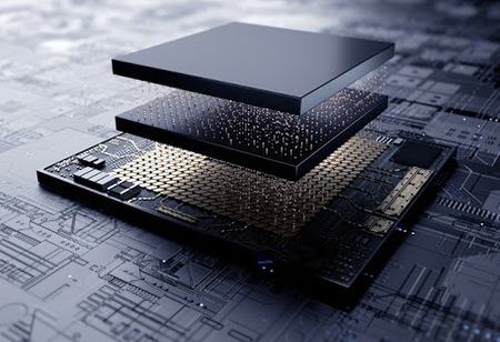
The heterogeneous integration technology of Samsung's I-Cube places one or more logic dies horizontally, such as central processing units (CPU) and graphics processing units (GPU), and several high bandwidth memory (HBM) dies on a paper-thin silicon interposer, which functions as a single chip in one package.
According to sources, it has built a unique mold-free structure for the I-Cube 4 solution, which incorporates four HBMs with one logic die, for better thermal management and stable power supply.
The yield obtained by I-Cube 4 solution with its pre-screening tests reduces the number of process steps to save costs and cut turnaround time.
As the zeal to explore new and better solutions has no deadline, Samsung is currently working on advanced chip packaging technologies to I-Cube 6 and higher to deal with interposer war page and thermal expansion through changes to material and thickness.